Repair Status: Repair still in progress. Last updated on 7/26/2026.
In for repair is a Namco System 2 arcade boardset with the Darksoft Namco System 2 Multi kit installed.
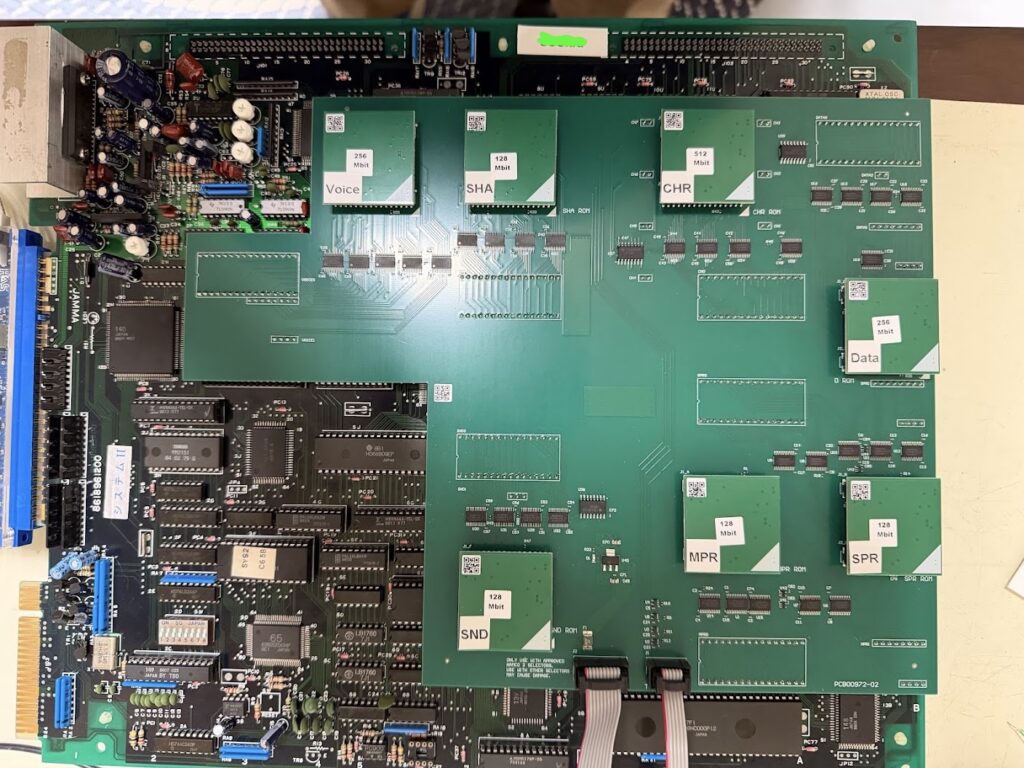
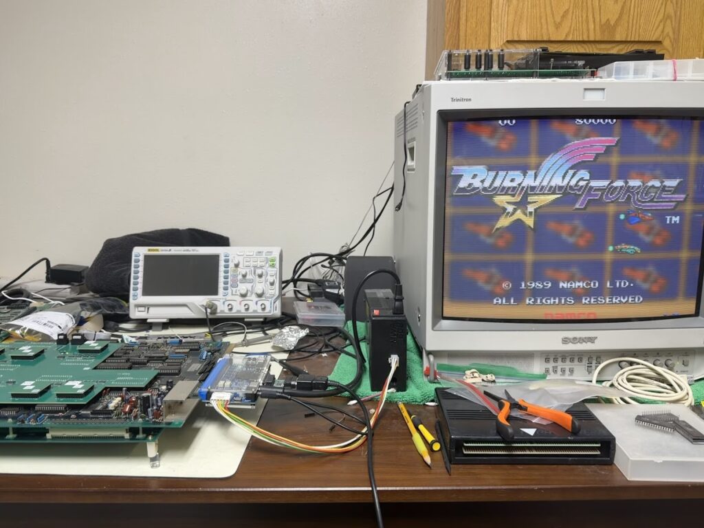
Namco System 2 was a powerful late-80s arcade system that hosted over 20 games. The majority of the games ran on a “standard” setup of a CPU board and a Video board, while a handful of titles utilized either an additional third daughterboard or a completely different video board. The Darksoft Multi installs onto the “standard” System 2 board set and thus allows you to run approximately 14 of the total games on one donor board.
I say “approximately” here because some System 2 games implemented a protection mechanism. Protected games used a so-called KeyCus chip that was unique to that game. If a protected game didn’t have a matching KeyCus chip then it wouldn’t boot up and run properly. Most (but not all) of the protected Namco System 2 games have had their protection mechanisms patched out by the enthusiast community. The Darksoft Multi doesn’t reproduce KeyCus behavior, so it requires that de-protected ROM sets be used.
The problem with this board set is that not all of the games supported by the Darksoft Multi kit would run properly. These games would run fine:
- Assault
- Assault Plus
- Burning Force
- Cosmo Gang
- Dragon Saber
- Finest Hour
- Super World Stadium ‘92
- Ordyne
- Rolling Thunder 2
- Legend of Valkyrie
- Marvel Land (USA Prototype)
While these games would hang on a black screen (with repeated audio clicks) or rapidly blink a blue screen at the end of the startup diagnostics:
- Marvel Land (Japan)
- Mirai Ninja
- Phelios
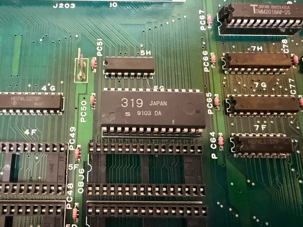
The donor game for this board set is the game Assault, and that game runs fine on the board, both with the factory ROMs and the Darksoft Multi. Assault did not utilize a KeyCus protection mechanism though, so the KeyCus socket at position 5G was left empty at the factory.
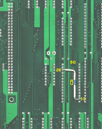
The Darksoft Multi instructions specify that either a KeyCus (any KeyCus) be installed in the 5G socket, or that a diode be installed between pins 13 and 26 on the socket. This board already had the diode installed correctly.
We’ll revisit the protection system shortly. First, I did some straightforward troubleshooting. I personally own a fully functional Namco System 2 board set (donor game was Rolling Thunder 2) with a Darksoft Multi kit also installed. By swapping the CPU and Video boards around between these two board sets, I was able to deduce that the project CPU board is fine and that the fault lies with the Video board.
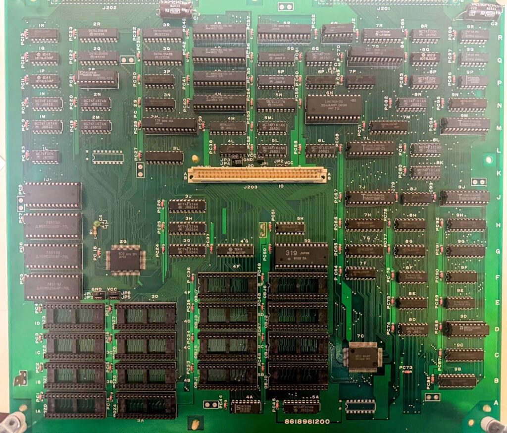
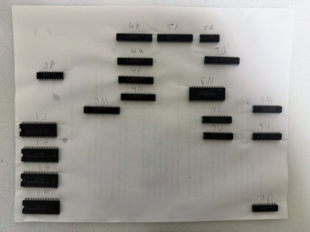
The Video board has several socketed components – mostly RAM and GAL chips. I removed and tested all of the RAM chips in a chip tester – all of them passed. I also tried exchanging all of the socketed components between the faulty video board and my working video board – and the behavior stayed the same. That meant that the fault on the video board was with something else besides the socketed components.
Now it’s time for advanced diagnostics. Thankfully, schematics for this board are available in the manual for the game Assault.
I decided to focus on the protection system next as the possible culprit. So what does that KeyCus diode bypass do? The schematics for the 5G KeyCus socket (labeled CUSXX on the schematics) show that Pin 13 is a signal called BUSACK and Pin 26 is a signal called KEY. Thus, the diode connects the KEY signal to the BUSACK signal. Both signals are prefixed on the schematic with a slash / , so they are Inactive when the signal holds High, and Active when they get pulled Low. BUSACK is the CPU Bus Acknowledge signal that tells the CPU when a subsystem has taken control of the bus. Since BUSACK is a shared signal, a diode is used instead of a bodge wire with the KeyCus bypass so that when BUSACK is triggered by another system component, that trigger doesn’t feed back into the KEY signal – the diode behaves as a “one way valve”.
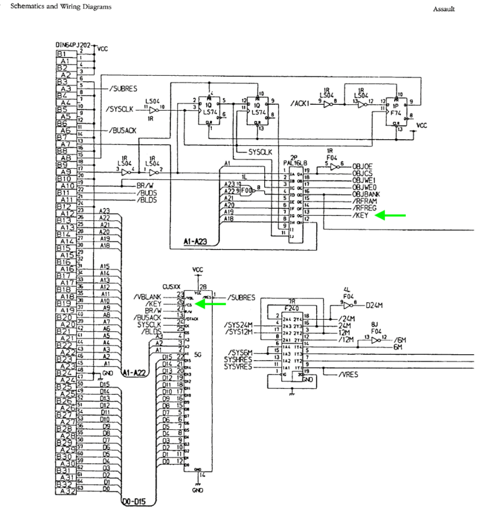
The same page of the schematics for the KeyCus socket also show that the KEY signal originates from a GAL chip located at position 2P on the board. I probed the KEY signal on the video board during the startup diagnostics for the non-booting games, and noticed it never triggers – the signal on the oscilloscope always reads High. Therefore, I made an assumption that the lack of a KEY signal trigger was the problem with those three non-booting games. [FYI: This assumption turned out to be incorrect, but I decided to explain the KEY diagnosis anyway for documentation purposes]
So … the GAL chip at location 2P doesn’t generate a KEY signal, and I know the GAL part itself is good because it’s a socketed part and the behavior stays the same when I swap in the same GAL from a fully functional Video board. A GAL chip acts like a switchboard – a set of conditions is programmed into the chip. When certain conditions are met, signals are switched High or Low for as long as the specified condition is met. In this scenario, KEY is Active Low, so the conditions in the GAL for that pin to toggle Low aren’t being met. But what are those conditions?
Fortunately, there is a straightforward way to find out. The GAL has been dumped, and by downloading the dump from the PLD Archive and decoding the JED file with the JEDUTIL application in MAME, we get these conditions:
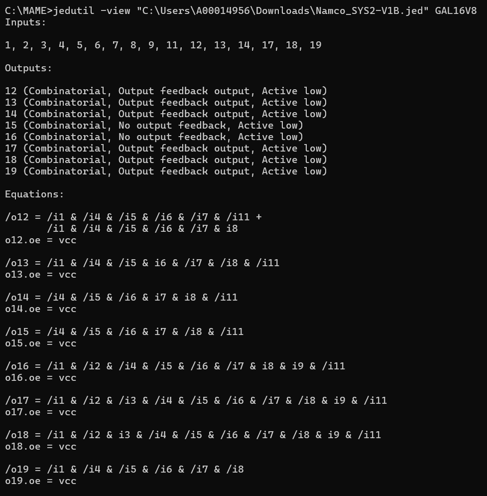
The KEY is on Pin 13 (o13), so for the KEY signal to trigger Low, the following must happen simultaneously:
- Pin 1 (i1): Must be LOW
- Pin 4 (i4): Must be LOW
- Pin 5 (i5): Must be LOW
- Pin 6 (i6): Must be HIGH
- Pin 7 (i7): Must be LOW
- Pin 8 (i8): Must be LOW
- Pin 11 (i11): Must be LOW
I started probing those pins on the faulty video board during the startup diagnostics for a non-functioning game. Pins 1, 4, 8 and 11 all showed healthy High / Low pulsing activity.
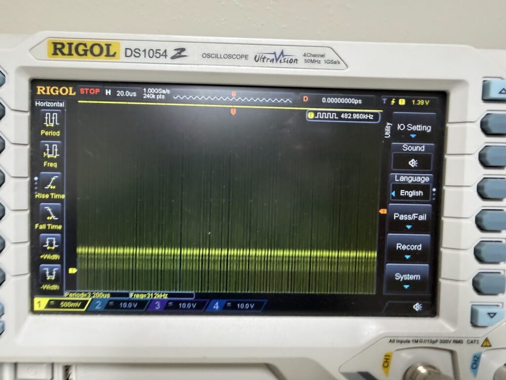
However, Pins 5 and 6 looked sickly – like they were trying to signal but the signals were getting pulled down. The scope’s maximum voltage for a pulse reading (VMax) was 1.14V, which is lower than the ~2.5V threshold the GAL has for treating a signal as High. Since Pins 5 and 6 never trigger High enough for the GAL, the KEY signal never gets triggered Low.
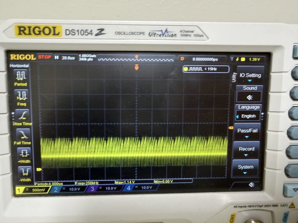
OK, so perhaps another part connected to GAL Pins 5 and 6 (such as a driver TTL) may have failed and is dragging those signals down. Let’s see what they are and what they connect to.
The schematics show that Pins 5 and 6 on the GAL are CPU Address lines A20 and A19, and that they come into the video board from the CPU board on Pins A13 and B14 of the connector labeled J202.
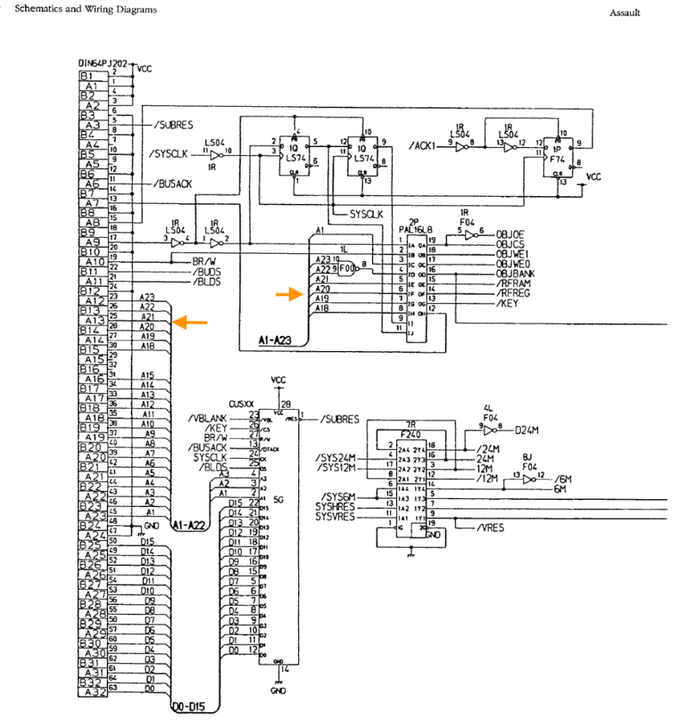
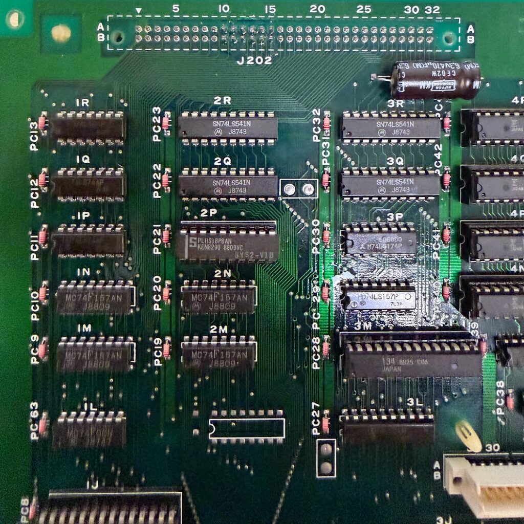
As much as I scoured the schematics though, I didn’t see those Address lines connecting to anything else on the Video board. Just to be certain, I used my multimeter in continuity mode and tested GAL Pins 5 and 6 against literally every other component pin on the Video board and found no other connections. Continuity tests from the GAL pins directly to the pins on the CPU board connector also showed a healthy connection.
As an experiment, I decided to bypass the video board connections for Pins 5 and 6 by bending them out of the GAL socket and soldering direct bodge wires from the pins to the CPU board. If this resolved the issue then I could look into a permanent fix.
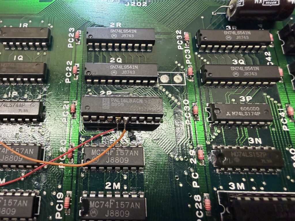
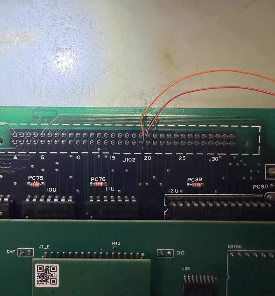
To my surprise, with this bypass in place, the scope readings were exactly the same – only 1.2V peak on High pulses. Physical connections weren’t the problem here.
At this point, I decided to go back to the Good video board and check the GAL signals there so I could compare and contrast. To my great surprise, the Good Video board showed identical behavior! I didn’t try every game, but on all of the games that the faulty Video board won’t run, on the Good Video board, the KEY signal never triggers Low and Pins 5 and 6 only show 1.2V peaks – until the game boots up, at which point Pin 5 shows healthy 5.1V peak High activity during screen transitions and Pin 6 never rises above 1.2V .
I’ve concluded that the low pulse readings I’ve been seeing on the scope for GAL Pins 5 and 6 are probably cross-talk interference from the nearby channels. The KEY signal never triggering has never been the cause of the faulty Video board to not run the games Marvel Land (Japan), Mirai Ninja and Phelios.
So, what to look at next? I know that the problem is presumebly still with one of the soldered components on the video board. I’m planning on checking as many of those components as I can with a diagnostic tool called SLICE. SLICE can monitor TTL logic chips in-circuit while the board is running and flag any aberrant behavior. Stay tuned!
PART 2
For the next round of troubleshooting, I broke out SLICE (Synchronic Live In Circuit Examiner) by GadgetFreak, a logic tester that monitors a TTL logic chip while it’s in operation and flags any circuit activity (toggles between High and Low pulses) that doesn’t match the specifications of the chip. SLICE is a both a software application and hardware clip that works in conjunction with a Digilent Discovery logic analyzer. Here is a link to the discussion thread on it in the UKVac Forums.
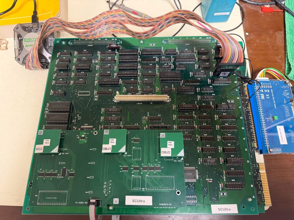
The hope is that SLICE will detect a bunch of logic errors on one of the soldered TTL logic chips on the video board, thus indicating a faulty chip that maybe hasn’t completely failed but is still “borderline” enough in its behavior that it would cause the bootup issues with Phelios, Marvel Land, and Mirai Ninja that I’m seeing with this board.
Overall, I used SLICE to check over 60 TTL logic chips on the video board. I took several samples of each chip as a game was running in different game states (ie title screen, gameplay, rotation & scaling layer active).
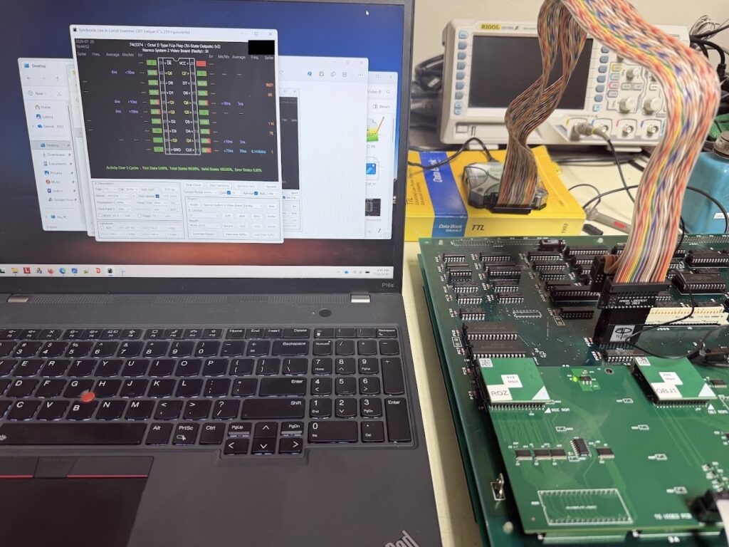
Almost all of the TTL parts tested as Good on every sample.
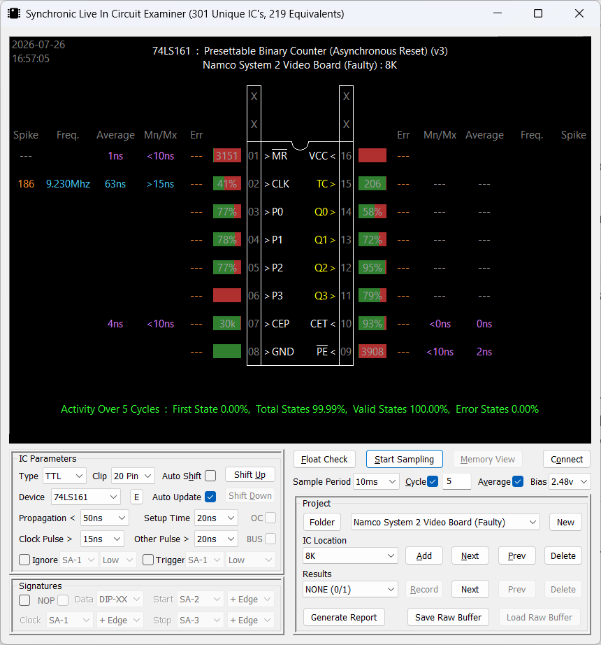
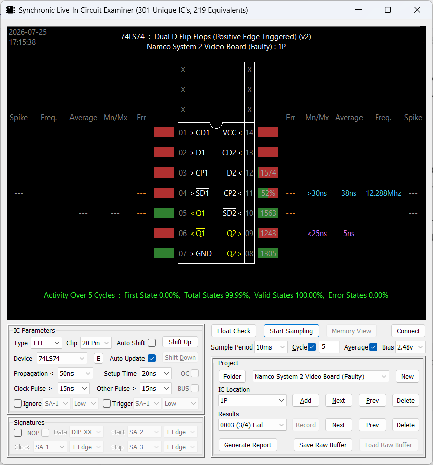
A few of the chips did register a small number of logic errors during the SLICE samples:
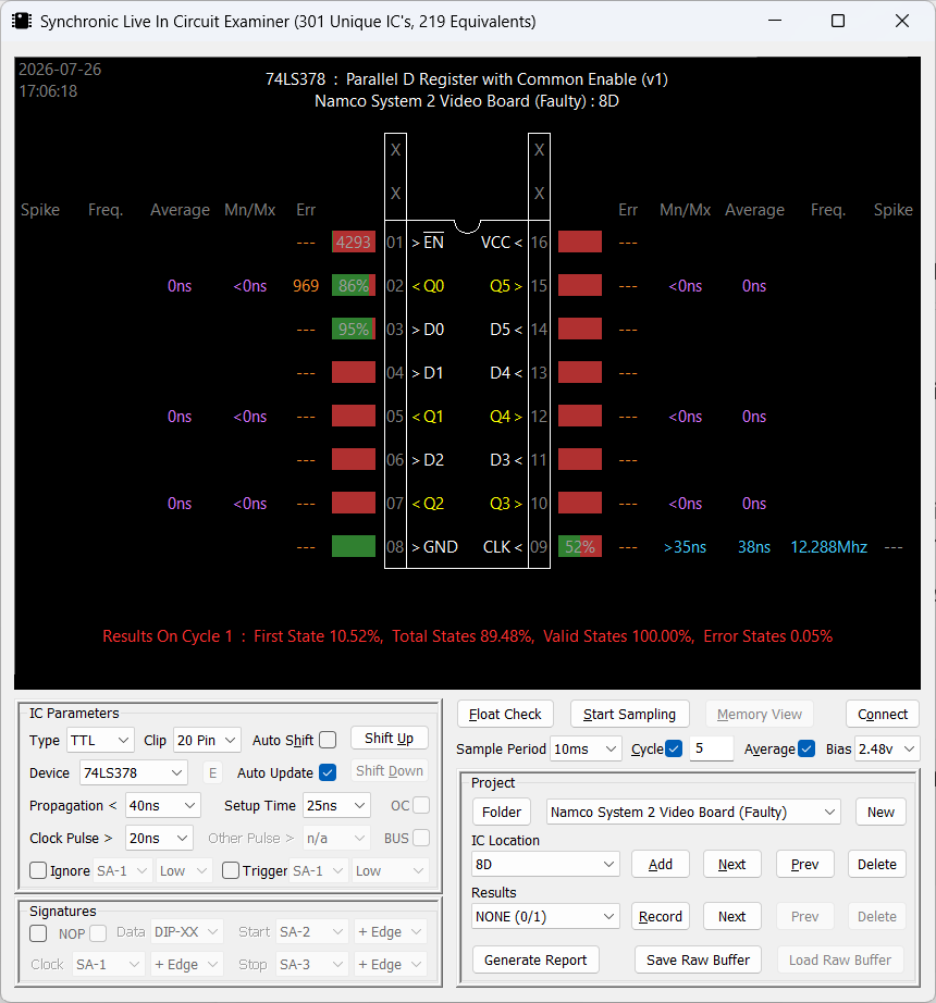
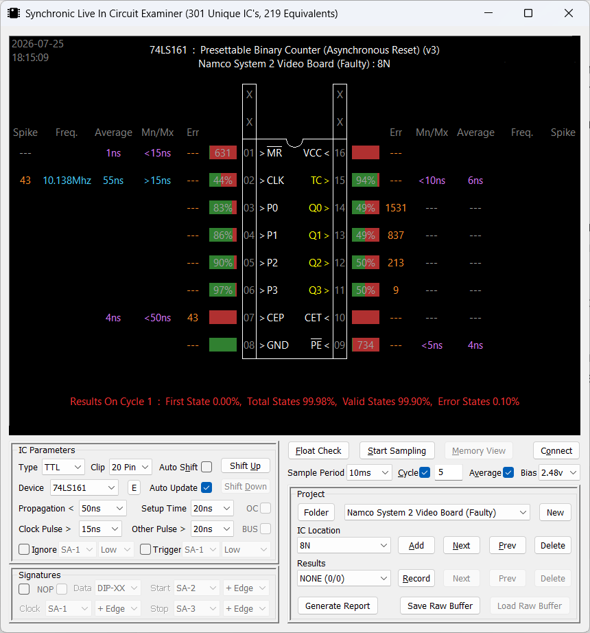
However, these suspect parts were likely fine and their logic errors were likely false positives. SLICE captures the signals through a clip that clips onto the chip being tested. Attaching the SLICE clip to the chip, adds a tiny bit of capacitive load to the pins. That added clip capacitance can cause ringing or signal bounce right at the moment the logic state flips. That very likely accounts for the small percentage of detected logic errors on these chips.
This MC74F175N part at location 6P was probably the most suspect of all the TTLs that I tested:
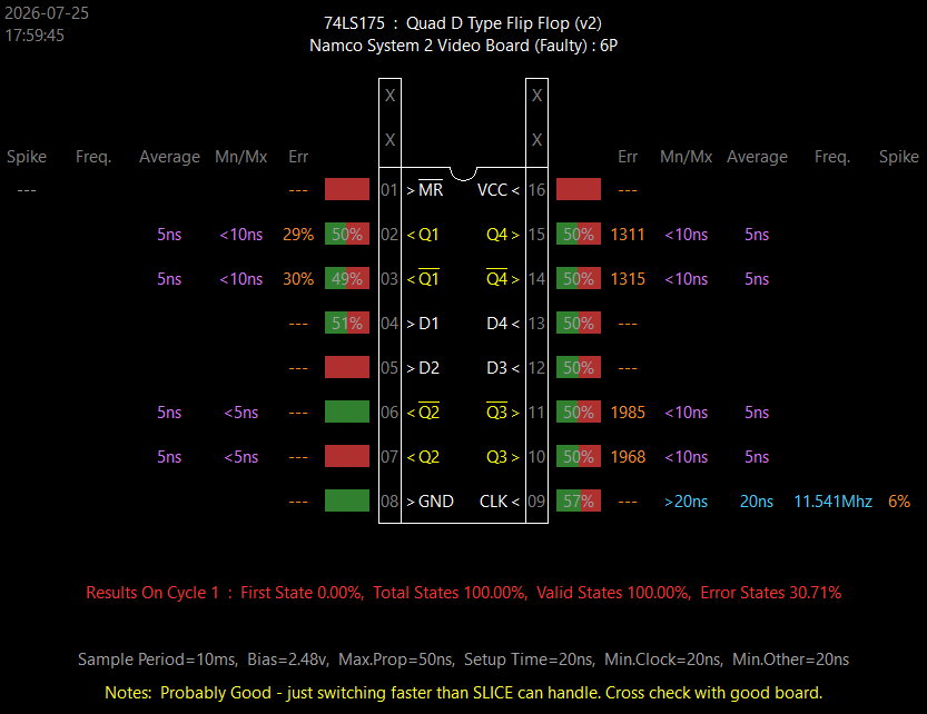
Some of the parts on the video board that deal with fast clock signals are high-speed F series (the F stands for Fast) parts such as the MC74F157AN. Although SLICE detected 30% logic errors on this part, it’s profiles are configured for the behavior of standard-speed LS series parts. Clock Pin 9 is switching at 11.541 mhz and the output pins 10, 11, 14 and 15 which are flagging errors are likely switching 2 – 3ns faster than SLICE’s 5ns scanning time. SLICE thus error flags some of the signal toggles that missed its detection window. So I concluded that this chip is also likely functioning properly.
After checking and confirming proper operation of all the soldered TTL parts, I’m reaching the end of the list on hardware issues I can diagnose in a timely fashion. As a recap, this is everything I’ve tried so far to resolve the issue of 3 out of 14 games not booting up on this System 2 board set:
- Isolated the fault to the video board and not the CPU board by swapping boards with a fully-functioning Namco System 2 board set.
- Confirmed that all socketed RAM was functional by testing the parts out-of-circuit in a RAM tester.
- Confirmed proper operation of all socketed parts (including RAM) by cross-swapping the socketed parts with the other Video Board.
- Confirmed proper operation of the Protection / KeyCus circuits by diagnosing their operation and comparing their behavior against the working board set.
- Confirmed proper operation of the soldered TTL logic chips by testing them in-circuit with the SLICE logic analyzer while a game was running.
I had one more idea that I wanted to try out – tackling the problem from the software side instead of the hardware side.
The three games that didn’t work would all run through the standard Namco system startup checks. These checks perform initial hardware setup, test the RAM, check the ROMs, etc. On the three nonfunctional games, after the tests the game would get stuck in a reset loop on the last screen of the startup tests – either a black screen or a blue box that would flicker repeatedly while the sound repeatedly clicked. Is it possible that if I hacked the ROMs to skip the startup checks and boot directly into the game (after hardware setup) that it would skip over whatever hardware quirk was hanging up those three games?
Although I have both an educational and professional day-job background in software engineering, it’s all in modern day technology and not the Motorola 68000 CPU assembly language that the Namco System 2 platform uses for both of its main CPUs.
However, I’ve always wanted to learn 68000 assembly, and I’m not adverse to using AI as an educated advisor as long as I’m the one still writing the code. I used the “trace” command in the MAME debugger to log all of the assembly instructions processed by the primary CPU during the startup diagnostics of each game. Then, with a lookup table of 68000 opcodes and some guidance from Google Gemini Pro in looking over the trace logs, I was able to successfully hack the ROMs to skip the startup diagnostics.
Here’s a quick video of the stock Phelios booting up:
And a quick video of the hacked Phelios booting up:
Phelios – Skip Startup Checks
Perform on 16-bit interleaved MPR ROM files
| ROM Address | Original Bytes | New Bytes (Patch) | Instruction Translation |
00025F34 | 66 34 | 60 34 | bra $25f6a |
00025F88 | 66 04 | 60 04 | bra $25f8e |
00025FA8 | 66 42 | 60 42 | bra $25fec |
00025FFE | 66 1C | 60 1C | bra $2601c |
Marvel Land – Skip Startup Checks
Perform on 16-bit interleaved MPR ROM files
| ROM Address | Original Bytes | New Bytes (Patch) | Instruction Translation |
00001E58 | 66 24 | 60 24 | bra $1e7e |
00001EAC | 66 04 | 60 04 | bra $1eb2 |
00001F28 | 66 04 | 60 04 | bra $1f2e |
00001F40 | 66 1C | 60 1C | bra $1f5e |
Mirai Ninja – Skip Startup Checks
Perform on 16-bit interleaved MPR ROM files
| ROM Address | Original Bytes | New Bytes (Patch) | Instruction Translation |
0001DD26 | 66 34 | 60 34 | bra $1dd5c |
0001DD7A | 66 04 | 60 04 | bra $1dd80 |
0001DD9A | 66 42 | 60 42 | bra $1ddde |
0001DDF0 | 66 1C | 60 1C | bra $1de0e |
When the Namco System 2 Multi first released, I wrote a Windows app for rolling up the individual game ROM sets into bundled files ready to be programmed onto the Multi’s flash modules. I loaded these new hacked ROMs into my rollup tool, built updated bundles, and flashed them onto the Multi’s flash modules.
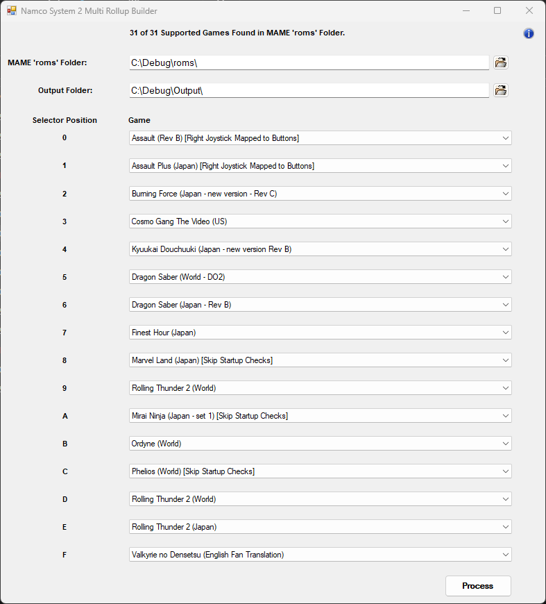
Unfortunately, skipping the startup diagnostics didn’t get those three games working on this video board either.
Next, I’ve been talking with some other arcade repair folks on Discord and they’ve offered some great suggestions on some further diagnostics I can try. Stay tuned!